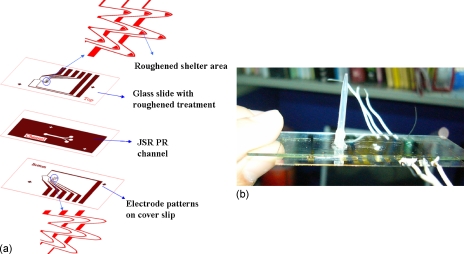
Figure 1.
(a) Chip design and construction. The electrode patterns of the bottom layer were fabricated on a thin cover slip slide and the electrode pattern of the top layer was fabricated on a treated glass slide. A roughened metal shelter was designed in front of the trapping electrode of the top layer that not only reduces the fluorescence noise but also enhances Raman signal. (b) Finished chip.

