
Figure 1.
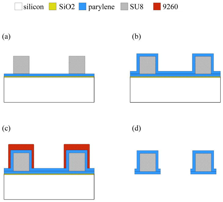
Cross-sectional view of wafer level fabrication. (a) Parylene deposited on SiO2 sacrificial layer and the SU-8 patterned shank. (b) Parylene encapsulated SU-8 structure. (c) 9260 resist patterned to form thick mask over shank. (d) Etched and released final structure. Photolithography masks used steps in (a, c).