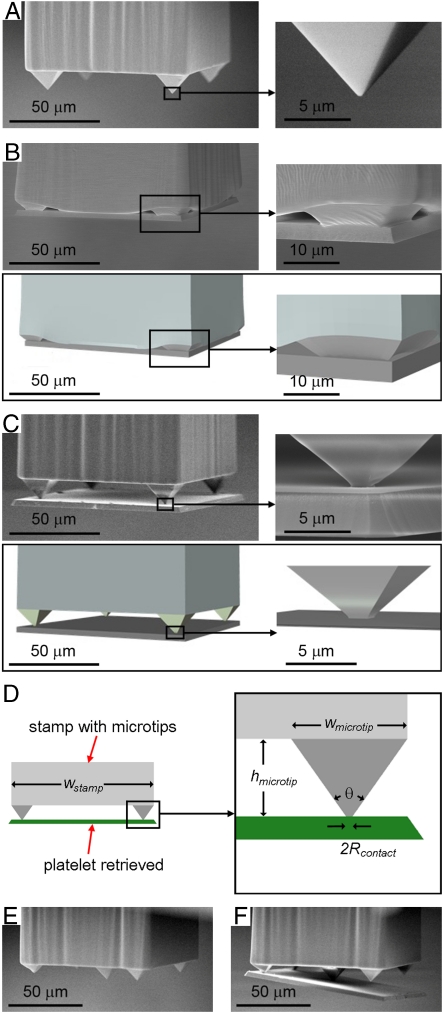
Fig. 2.
SEM and FEM images of representative elastomeric stamps in microtip designs, with and without silicon platelets (3 μm thick; 100 × 100 μm) on their surfaces. (A–C) Four-tipped layout. The right frames provide magnified views of one of the microtips and the bottom frames provide corresponding images of the results of finite element modeling (B, C). (D) Schematic illustration for notation of the stamp dimension. (E, F) Five-tipped layout. In this design, the silicon platelet remains in contact only with the largest, central microtip in the final stages of the transfer printing process.

