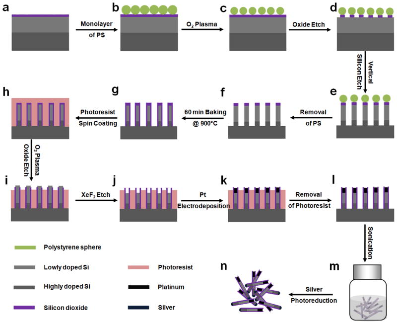
Figure 2.
Schematic illustration of the synthesis of Pt/Si/Ag nanowire photodiodes. (a) The starting n/n+ silicon wafer with a 360 nm silicon oxide. (b) Formation of close-packed monolayer of polystyrene (PS) spheres by a drop casting method. (c) Formation of non-close-packed monolayer of PS spheres by O2 plasma. (d) Formation of the patterned DRIE etching-mask containing PS spheres and the underneath silicon oxide discs obtained from using an AOE oxide etching recipe. (e) Using DRIE to obtain vertical Si nanowire arrays. (f) Removal of PS spheres and the residue in chloroform and hydrofluoric acid solution. (g) Formation of silicon oxide shell on Si nanowires by baking sample under ambient conditions at 900 °C for 60 min. (h) Spin coating of photoresist AZ 5214 as a protecting layer for the substrate. (i) Exposure of the Si core of the silicon oxide-encased Si nanowires through an O2 plasma process followed by oxide dry etching. j. Drilling of the nanoholes in the Si nanowires by XeF2 dry etching. (k) Pt electrodeposition. l, Removal of photoresist AZ 5214. m, Release of Pt/Si nanowires into solvent through sonication. (n) Self-catalyzed photoreduction of silver by irradiation on freshly released Pt/Si nanowires in AgNO3 aqueous solution.

