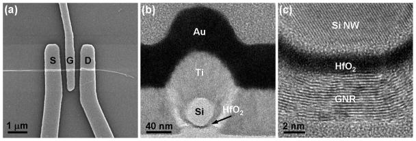
Fig. 3.
Characterization of the graphene/HfO2 interface. (a) A SEM image of a typical device. (b) A cross-section TEM image of the top gate stack. (c) A cross-section HRTEM image of the interface between nanowires and a multi-layers graphene, which indicate that the graphene layers are intimately integrated with the Si/HfO2 nanowire without any obvious gap or impurities between them. A TEM image of multi-layer graphene device is shown here because it is very difficult to visualize the mono- or few-layer of graphene nanoribbon under the nanowire due to significant electron-beam damage while conducting TEM studies.

