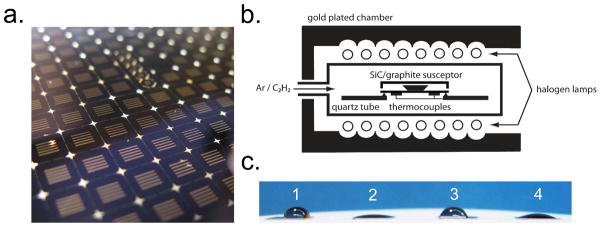
Figure 1.
Preparation of carbonized membranes. (a) Porous nanocrystalline silicon membrane chips fabricated on a 4-inch wafer. The active membrane area appears as five slits in the middle of the bulk silicon scaffold. The ultrathin porous nanocrystalline silicon membrane is 15 nm thick. (b) Schematic of the rapid thermal processing unit used for carbonization. Membrane chips are placed inside a SiC coated graphite susceptor. A mixture of argon and acetylene is introduced into the chamber and heated to high temperatures. Two thermocouples monitor the temperature uniformity of the process. (c) (1) Contact angles of an untreated (76°), (2) ozone treated (16°), (3) carbonized (60°), and (4) carbonized and ozone treated (22°) membrane.

