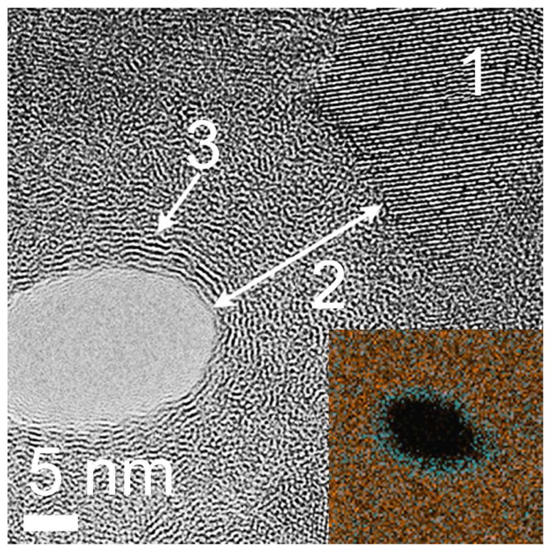
Figure 4.

High-resolution bright field TEM images of a carbonized pore. The inset shows an x-ray energy dispersive x-ray (EDX) scan of a single carbonized pore. The EDX scan highlights areas of Si (red) and C (blue) composition. Label 1 marks a <111> oriented Si nanocrystal at the perimeter of the original pore wall. The carbon layer is highlighted by the arrow (2). Atomic ordering can be seen far from the original pore wall consistent with the spacing (3.6 Å) between sheets of graphite (3).
