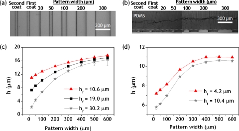
Figure 3.
Thickness variation of patterned microchannel features fabricated by two-step photolithography. (a) Optical top-view image of multilevel microchannels molded in PDMS. The first and second coats refer to the first and second PR coating layers, respectively. The layer thicknesses were hf=30.2 μm andhs=20.1 μm. (b) Optical cross-sectional image of the microchannels. (c) Measurements of h vs pattern width. The second layer thickness hs for all cases was fixed at 20.1 μm on average, while the first layer thickness varied from 10.6 to30.2 μm. (d) Measurements of h vs pattern width. The second layer thickness hs for all cases was fixed at 10.8 μm on average, while the first layer thickness varied from 4.2 to10.4 μm.

