
Figure 6.
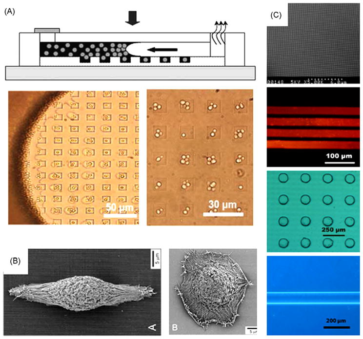
Substrate physical patterning. (A) Top: schematic of cell docking in microwells using capillary force. Down: picture of SG3 yeast docking in microwells [83]. (B) Cell guidance using physically modified substrate. Left: picture of corneal epithelial cells on SiO2 substrate with 70 nm wide ridges. Right: cell on a smooth SiO2 substrate [91]. (C) Example of pattern made by micromolding technique. From top to bottom: 150 nm diameter pillar, fluorescent image of 40 μm stripe of quantum dot, 100 μm hole in a 20 μm thick PDMS layer, optical image of 100 μm width and 20 μm height wall of agar gel [84].