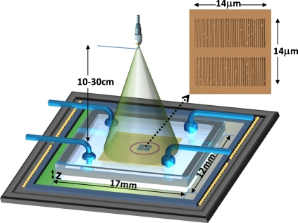
Figure 1.
Lensfree on-chip sensing setup. A plasmonic nanoaperture array, as shown in the SEM image on the top right corner, is illuminated with a quasimonochromatic source (e.g., 550 nm center wavelength with ∼20 nm bandwidth) located ∼10–30 cm away from its surface. The lensfree transmission pattern of this plasmonic structure is sampled by a CMOS chip placed at z∼1 mm away from the aperture plane. The yellow surface indicates the detector active area (∼6×4 mm2). The plasmonic nanoaperture array shown above is composed of uniformly spaced slits each with a length of ∼6 μm where the slit width varied (from left to right) between ∼80 and ∼200 nm in discrete steps of ∼20 nm. The physical gap between two neighboring slits is kept constant at ∼200 nm.

