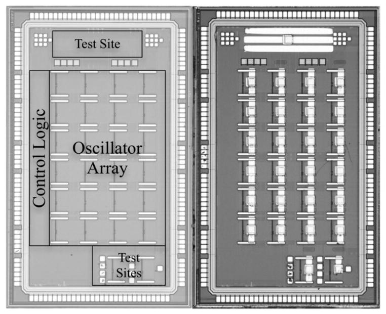
Figure 4.

Left die photo shows CMOS as returned from foundry. Boxes indicate layout of underlying CMOS architecture. Right die photo shows chip after fabrication of FBAR structures, including the passive test structure along the top edge.

Left die photo shows CMOS as returned from foundry. Boxes indicate layout of underlying CMOS architecture. Right die photo shows chip after fabrication of FBAR structures, including the passive test structure along the top edge.