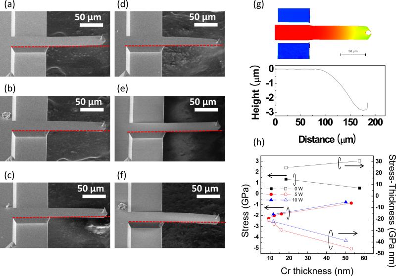
Figure 2.
(a) – (d) SEM images of the cantilevers as a function of substrate bias and Cr thin film thickness; (a) 0 W substrate bias, 18.4 nm, (b) 5 W substrate bias, 12.2 nm, (c) 10 W substrate bias, 11.7 nm, (d) 5 W substrate bias, 16.0 nm, and (e) – (f) SEM images of the cantilevers after 138 nm-thick PECVD SiO2 deposition with Cr film of (e) 0 W substrate bias, 18.4 nm and (f) 5 W substrate bias, 12.2 nm. (g) Typical top-view optical micrograph and profilometer scan for the cantilever with 5 W substrate biased Cr thin film, (h) Cr film stress (solid symbol), and product of stress-thickness (open symbol) as a function of Cr thickness at 0, 5, and 10 W substrate bias.

