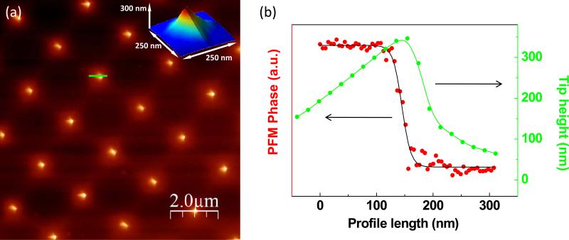
Figure 7.
(a) Tapping mode AFM image of the standard grid of sharp spikes (Inset: three-dimensional representation of tip shape). (b) Topography line profile (green line in figure 9 (a)) and PFM phase line profile (red line in figure 10). Tip radius obtained from topography profile (~ 30 nm) corresponds well with tip radius (32 nm) obtained from PFM phase fitting.

