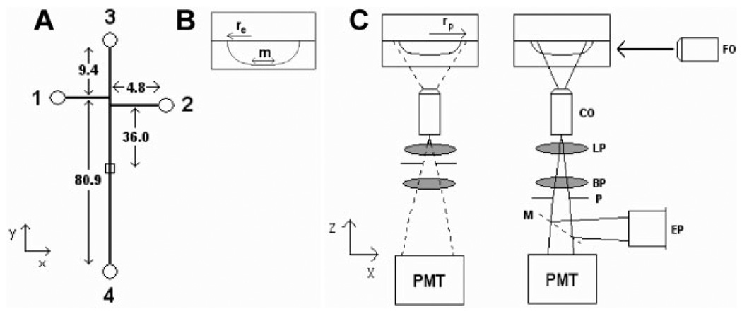
Figure 1.
Schematic diagram of microfluidic devices and orthogonal fluorescence detection scheme. (A) 1, 2, 3, and 4 represent the sample, sample waste, buffer, and buffer waste reservoirs, respectively, with a detection zone 36.0 mm from the channel intersection. All distances are given in mm. (B) Channel dimensions as defined by the etch depth (re = 20 µm) and the mask width (m = 10 µm). (C) Laser light is focused onto the microfluidic device with a 6.3× objective (FO), fluorescence is collected with a 60× long working distance objective (CO), passed through a 505 nm long pass filter (LP), a 535 ± 17 nm bandbass filter (BP), and a pinhole (P) before being detected by the photo-multiplier tube (PMT). The pinhole produces a collection zone (rp) defined by the position of the pinhole in the detector. Alternately, a mirror (M) could redirect the fluorescence to an eyepiece (EP) for rough alignment. The pinhole is placed at either 47 or 66 mm from the back of the collection objective so that light is collected from a zone on the device with a radius of either 27.8 or 19.8 µm.

