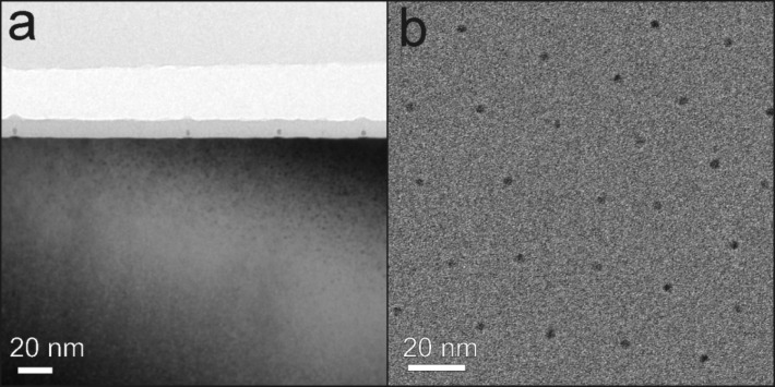
Figure 7.
TEM images of 3 nm FePt NPs on Si/SiO2 after annealing at 650 °C for 90 min. (a) Bright-field TEM image of FePt nanoparticles in cross section view. The NPs are in situ covered by a thin layer (10 nm) of SiO2 to avoid oxidation and mechanical damage after annealing. (b) Bright-field TEM image of FePt NPs in plane view. The hexagonal ordering can be clearly seen.

