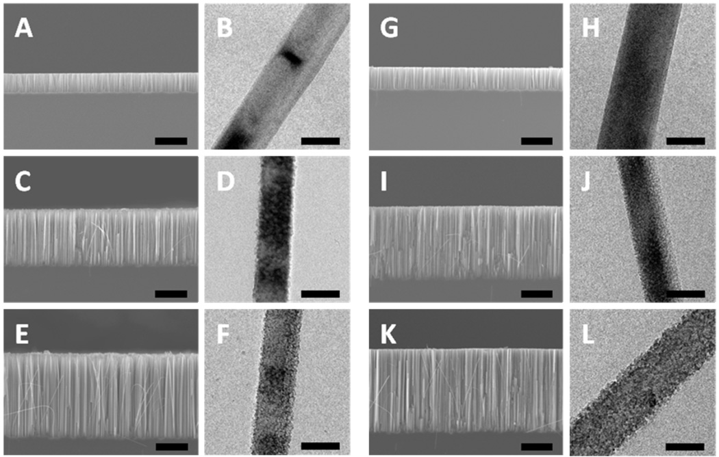
Figure 1.
TEM and SEM images of the silicon nanowires obtained from 1–5 and 0.3–0.8 Ω·cm n-type Si (100) wafer in etchant solutions composed of 4.8 M HF and H2O2 of variable concentrations through a two-step reaction for 30 minutes. (A,B) Nanowires formed from 1–5 Ω·cm silicon wafer with 0.1 M H2O2. (C,D) Nanowires formed from 1–5 Ω·cm silicon wafer with 0.3 M H2O2. (E,F) Nanowires formed from 1–5 Ω·cm silicon wafer with 0.6 M H2O2. (G,H) Nanowires formed from 0.3–0.8 Ω·cm silicon wafer with 0.1 M H2O2. (I,J) Nanowires formed from 0.3–0.8 Ω·cm silicon wafer with 0.3 M H2O2. (K,L) Nanowires formed from 0.3–0.8 Ω·cm silicon wafer with 0.6M H2O2. The scale bars in all SEM and TEM images are 10 µm and 100 nm, respectively.

