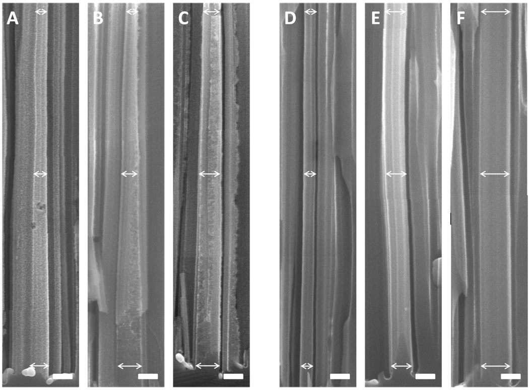
Figure 10.
(A–C) Cross sectional SEM images of nanowires from 0.008–0.016 Ω·cm silicon wafer etched in 0.3 M H2O2 for 15 mintues, showing the trapezoid structure. The diameter of the upper part is smaller than the lower part, indicating the size of Ag nanoparticle is shrinking as the reaction proceeds. (D–F) Cross sectional SEM images of nanowires from 0.3–0.8 Ω·cm silicon wafer etched in 0.3 M H2O2 for 15 mintues, showing nearly constant wire width/diameter, suggesting that the size of Ag nanoparticles remains nearly unchanged in the etching process. The images are grouped together from multiple images to show the diameter/width evolution over extended length. The scale bars are 200 nm.

