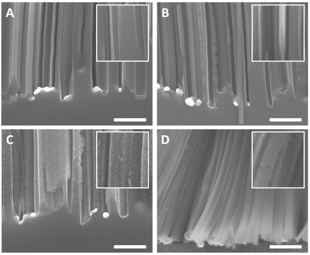
Figure 7.
Cross sectional SEM image of nanowires evolved from four types wafers with reaction time of 15 minutes in the etchant solutions containing 0.3 M H2O2 without immersing in the nitric acid solution. The insets are enlarged SEM images for each type of the nanowires respectively. (A) Silicon nanowires from 1–5 Ω·cm wafer. (B) Silicon nanowires from 0.3–0.8 Ω·cm wafer. (C) Silicon nanowires from 0.008–0.016 Ω·cm wafer. (D) Silicon nanowires from 0.001–0.002 Ω·cm wafer. The scale bars are 500 nm.

