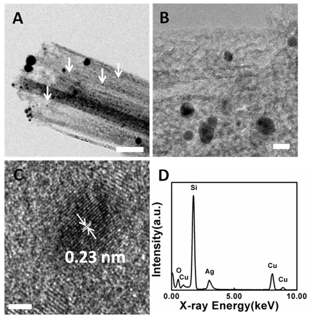
Figure 8.
(A,B) TEM images of a porous silicon nanowire decorated with Ag nanoparticles on the sidewall. The silicon nanowire was made from 0.008–0.016 Ω·cm silicon wafer in 0.3 M H2O2 for 15 minutes without the treatment in the concentrated nitric acid. Small Ag nanoparticles are indicated by the white arrows. The scale bars are 80 nm and 20 nm for 8A and 8B, respectively. (C) HRTEM of Ag nanoparticles on the sidewall of the porous silicon nanowire. The lattice spacing 0.23 nm corresponds to Ag (111) plane. The scale bar is 2 nm. (D) An EDX spectrum recorded from one nanowire. Ag was detected on the nanowire, confirming the TEM characterization.

