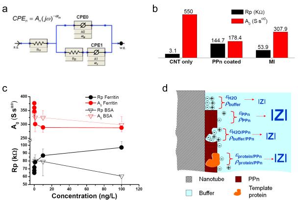
Figure 3.
Detection mechanism of the molecular imprint nanosensor. a, Equivalent circuit model with constant phase elements (CPE). b, Rp and A0 derived from Nyquist plots fittings at various fabrication stages corresponding to: nanotube tips devoid of PPn (CNT only), nanotube tips coated with template protein entrapped PPn (PPn coated), and template protein molecular imprinted nanotube tips (MI). c, Rp and A0 vs. hFtn or BSA concentrations; error bars show standard error of the mean (n=3). d, Four scenarios of sensor surface conditions closely related to resistivity (ρ) and permittivity (ε): 1) bare nanotube surface, where solution double-layer dominates the surface, (εH2O, ρbuffer); 2) nanotube surface coated by PPn, (εPPn, ρPPn); 3) nanotube coated by PPn with imprint sites, (εH2O/PPn, ρbuffer/PPn); and 4) imprint sites occupied with re-bound template protein, (εprotein/PPn, ρprotein/PPn).

