Figure 3.
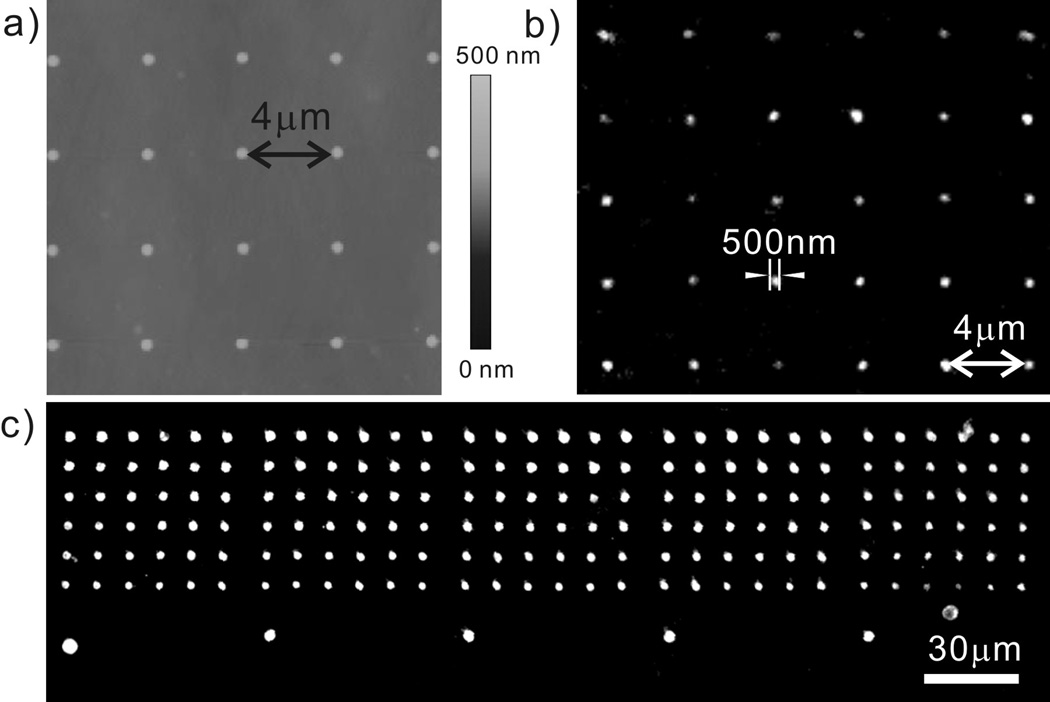
(a) An AFM topography of the PEG pattern used for fabricating a flat stamp for μCP of proteins. (b) A fluorescent image of the printed TRITC conjugated anti-mouse IgG. (c) A fluorescent image of the printed TRITC pattern on glass.
The intrinsic drawbacks in conventional microcontact printing, i.e. roof collapse and lateral ink diffusion, were addressed by using topographically flat, chemically patterned PDMS stamps made by Dip-Pen Nanolithography (DPN). The chemically patterned flat stamps were used for contact printing of various inks including thiols, proteins and hydrophilic dyes. The as-made features can reach sub-100 nm resolution and very low filling factor (<1/100).##DPN benefits μCP
dip-pen nanolithography
microcontact printing
silanes
nanofabrication
surface chemistry

