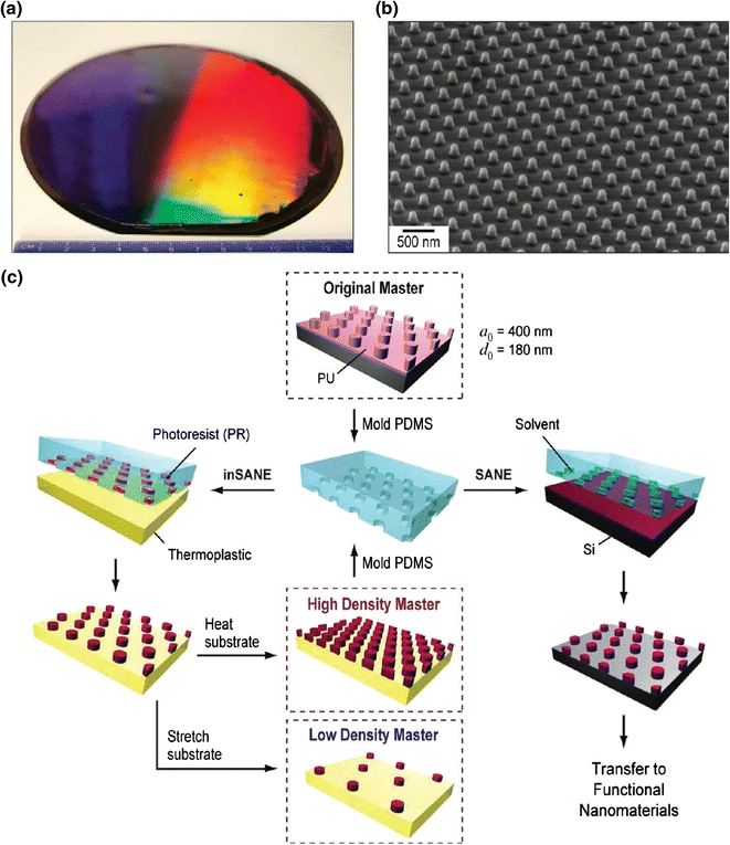
Figure 5.

Schematic of solvent-assisted nanoscale embossing. (a) Optical micrograph of PU master; (6 in) diameter; (b) SEM images of nano-structures on PU master; (c) Schematic of inverse SANE (inSANE) fabrication procedure for the generation of high and low density nanostructures. Figure reprinted with permission from Lee et al. 52
