
Figure 1.
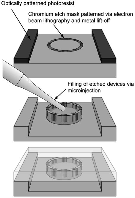
Fabrication of nanoporous reaction vessels within microfluidic channels is carried out by combining electron beam lithography and metal lift-off techniques with contact photolithography to define the reaction vessel and channel geometries (top). The pattern is transferred into the exposed silicon using cryogenic silicon etching and individual vessels are filled with reactants via microinjection (middle). Whole chips are then sealed with a silicone elastomer lid (bottom)