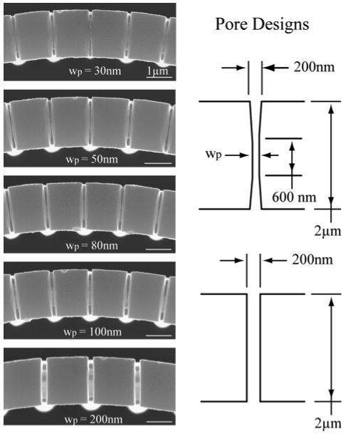
Figure 3.

Top view scanning electron micrographs of the porous membranes taken at a magnification of 35000X show the different dimension pores achieved via electron beam lithography and cryogenic silicon etching. Pore width (wp), corresponds to the dimension used in the lithography patterns. Final dimensions ranged from approximately 10 to 30nm smaller than the CAD-defined pore width.
