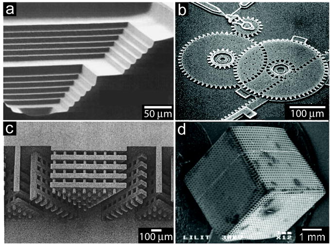
Figure 2. Structures fabricated using masked lithography.

a) SEM of a structure with step sizes of 10 and 30 μm etched into a silicon substrate. b) Interdigitated gears of a multilayer microtransmission fabricated using surface micromachining. c) UV-LIGA-fabricated PMMA microstructures exposed to two angled irradiations. d) 3D PMMA scaffold made using X-ray lithography.
Reproduced with permission from Reference [41]. Copyright 1998, IEEE. b) Courtesy of Sandia National Laboratories, Reference [188]. c) Reproduced with permission from Reference [49]. Copyright 1998, American Institute of Physics. d) Reproduced with permission from Reference [55]. Copyright 2006, IOP Publishing.
