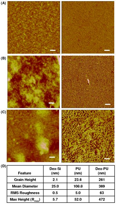
Figure 2.
AFM images of dry (A) dextranized silicon, (B) PU film, and (C) dextranized PU film. The scanning sizes are 1 × 1 μm2 for dextranized silicon, and 5 × 5 μm2 for PU film and dextranized PU film. The scale bars are 100 nm for dextranized silicon, and 500 nm for PU film and dextranized PU film. The left and right images are topographical and phase data, respectively. (D) Quantitative analysis of the surface roughness.

