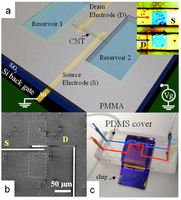
Figure 1.
Measurement of a SWCNT nanofluidic channel integrated with a SWCNT field effect transistor. (a) Schematic of the device structure and electrical measurement configuration. The inset shows an optical image of a device. The two blue squares (i.e., 60 μm × 60 μm) are the fluid reservoirs cut into the PMMA (yellow). Areas contacted by the PDMS cover are shown in green. Fluid flow in the PDMS channels is indicated by the red and blue arrows. The distance between source (S) and drain (D) electrodes (red) is 15μm. (b) Scanning electron microscopy (SEM) image of a single reservoir device after stripping off the PMMA layer to show the SWCNT lying under the electrodes. The areas labeled by the gray dashed squares indicate the position of the reservoirs. (c) Optical image of a device assembled with a PDMS cover for solution delivery. The read and blue lines show the fluid paths.

