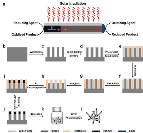
Figure 1.

Schematic illustration of the synthesis of Pt/Si/Ag nanowire heterostructures. (a) Schematic illustration of a metal-semiconductor-metal photoelectric nanodevice as a highly efficient photocatalyst. A Pt/n-Si/Ag heterostructure is created in a single nanowire to integrate a nanoscale metal-semiconductor Schottky photodiode (Pt-Si) encased in a protective insulating shell with two exposed metal catalysts (Pt, Ag). (b) The starting lightly doped silicon wafer. (c) Formation of silicon nanowire arrays by silver-assisted electroless wet chemical etching. (d) Formation of silicon oxide shell on Si nanowires by baking the sample under ambient conditions at 900 °C for 60 min. (e) Spin coating of photoresist AZ 5214 as a protecting layer for the substrate. (f) Exposure of the tips of the silicon nanowires through O2 plasma etching. (g) Exposure of the Si core of the silicon oxide-encased Si nanowires by oxide dry etching. (h) Drilling of the nanoholes in the Si nanowires by XeF2 dry etching. (i) Pt electrodeposition. (j) Removal of photoresist AZ 5214. (k) Release of Pt/Si nanowires into solvent through sonication. (l) Self-catalyzed photoreduction of silver by irradiation on freshly released Pt/Si nanowires in AgNO3 aqueous solution.
