Figure 2.
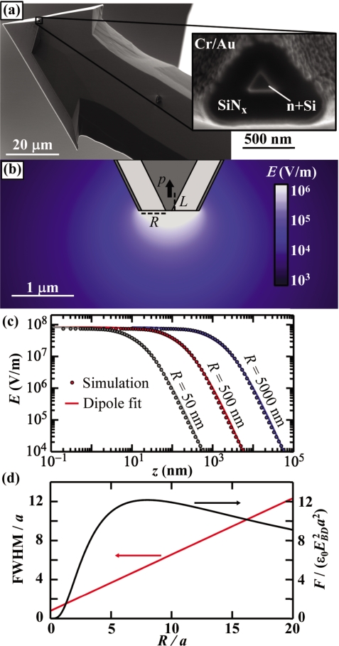
(a) Scanning electron micrograph of a typical coaxial AFM probe with (inset) a zoomed in view of the coaxial tip. The inner n+silicon conductor is surrounded by ∼400 nm of low stress silicon nitride and a Cr/Au ground shield. (b) Axially symmetric finite element electrostatic simulation of electric field of a coaxial probe. The inner conductor is held at 1 V and the outer conductor is grounded. (c) Simulated axial electric field of three coaxial probes with varying insulator thickness R. The voltage of each is scaled to set the maximum electric field strength to the dielectric breakdown field EBD of air. Each field profile is fit to a dipolar electric field. (b) Resolution vs sensitivity of coaxial probes. Left axis: the FWHM of the force as measured from probes with varying R. Right axis: maximum force exerted on a coaxial probe by a dielectric sphere directly below the probe. The maxima at R≈8a indicates an optimal R to detect a given object.

