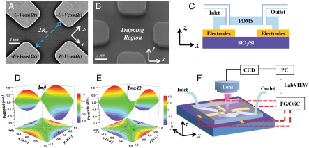
Fig. 1.
PAPT devices and experimental platform. (A) SEM of PAPT devices before integration with a microfluidic interface. The ac/dc voltages are applied such that the potentials of any two adjacent electrodes are of same magnitude but opposite sign. The physical size of the device is denoted 2R0. (B) Finely controlled processing results in smooth sidewalls of the electrodes, which helps to minimize the stray electric fields. (C) Sketch of a functional device with microfluidics integrated (not drawn to scale). PDMS, polydimethylsiloxane. (D and E) Illustration of working principles for the device shown in A under a pure ac case (U = 0). The x and y axes are normalized by R0. The z axis is normalized by V. At t = 0, the resulting electric forces (dashed arrows) will focus positively charged particles along the y direction and defocus them along the x direction. Half an rf period later, the potential polarity is reversed and opposite electric forces are thus generated. If the ac potential changes at the right frequency, the charged particles become stuck in this rapid back-and-forth motion. (F) Schematic of the experimental setup. The whole setup is built around a microscope. A LabVIEW (National Instruments) program controls the function generator (FG) to create the ac/dc voltages. The real voltage applied to the device is measured by an oscilloscope (OSC) and recorded by the same LabVIEW program. The electrical connections are through Bayonet Neill-Concelman cables (dashed lines). The videos taken by CCD are stored in personal computer (PC) memory in real time.

