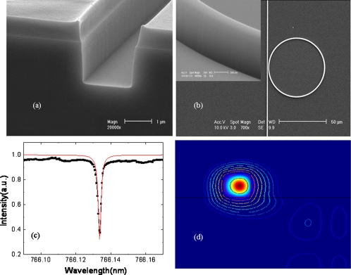
Figure 1.
(a) SEM picture of the silicon trench mold fabricated using optimized fabrication process showing smooth sidewalls, (b) SEM picture of an imprinted polymer microring coupled with a straight waveguide, and inset shows the sidewall of the imprinted polymer microring, (c) normalized transmission spectrum of polymer microring with D=60 μm, and (d) simulated electrical field intensity distribution a polymer microring waveguide with D=60 μm.

