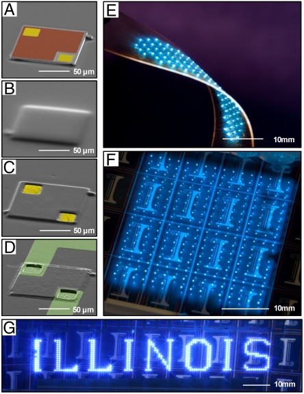
Fig. 2.
SEM images of the interconnection process for a representative InGaN μ-ILED, shown in sequence, (A) after assembly onto a optically transparent substrate (e.g., glass or plastic), (B) after spin-coating a photo-sensitive polymer, (C) after self-aligned via formation using a BSE process, and (D) after deposition and patterning of a metallic interconnect layer. The colorized regions correspond to the contact pads (gold), a thin current spreading layer (red), and Al interconnects (green). Optical images of various lighting modules based on arrays of μ-ILEDs (E) plastic and (F, G) glass substrates.

