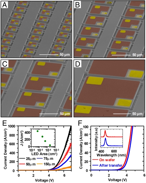
Fig. 3.
SEM images of arrays of released InGaN μ-ILEDs with dimensions from (A) 25 × 25 μm2, (B) 50 × 50 μm2, (C) 75 × 75 μm2 to (D) 150 × 150 μm2. The colorized regions correspond to the contact pads (gold), and thin current spreading layers (red). (E) Corresponding current density-voltage (J-V) characteristics for μ-ILEDs with the dimensions shown in (A). The inset provides a plot of current density as a function of μ-ILED area, measured at 6 V. (F) Current density-voltage (J-V) characteristics and emission spectrum (inset) of a representative device before undercut etching on the Si wafer, and after assembly onto a glass substrate.

