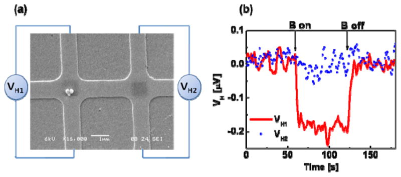
Figure 5.

(a) SEM image of a micro-Hall device that was patterned from an InAs QW wafer via photolithography and wet etching, then coated with an insulating layer of SiO2, followed by a Au layer for molecular interfacing. MHA was patterned by DPN (figure 4), then biotinylated (figure 2), and is evident as dark squares in the central, active regions of the Hall crosses; the surrounding Au surface was passivated with ODT (figure 2). Three streptavidin-coated magnetic beads assembled on the biotinylated region of the left cross. (b) ac Hall voltage as a function of time for the two crosses shown in (a). Due to the presence of magnetic beads on the left cross, the ac Hall voltage VH1 (red) decreased by ~0.19 μV when a dc magnetic field B = 70.6 mT was applied. In contrast, no change in Hall voltage VH2 (blue) was observed when B was applied to the empty cross.
