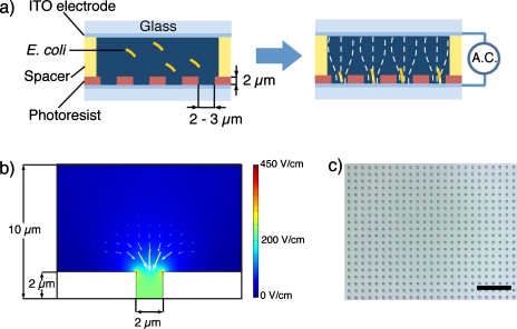
Figure 1.
(a) Schematic image of the single-cell trapping and lysing device. The solution containing target cells is introduced through the gap between the electrodes by capillary flow. The distance between the top and the bottom electrodes is kept about 100 μm with the spacer. A highly localized electric field, caused by the through-hole photoresist structure, efficiently induces DEP force to trap cells. Microwell structure having comparable size to the target cell allows single-cell trapping. (b) Simulated electric field with finite element method, where the electric potential, 1 V, is applied between top and bottom lines, and the permittivity of medium and microwell structure (white area) are 80.4 ε0 and 3.0 ε0 (ε0: vacuum permittivity), respectively. Color scheme shows the electric field strength from blue (lowest) to red (highest). White arrows represent ∇E2 indicating the direction of pDEP force. (c) Arrayed microwells patterned on the plane ITO electrode. The distance between center to center of each microwell is 10 μm. Large array of microwells will allow high-throughput single-cell analysis. Scale bar is 50 μm.

