
Fig. 1.
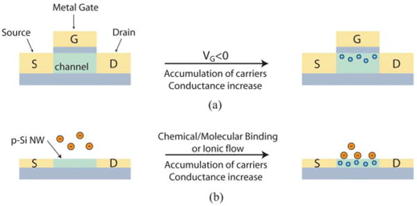
(a) Schematic of a p-type planar FET device, where S, D, and G correspond to source, drain and gate electrodes, respectively. (b) Schematic of electrically based sensing using a p-type NWFET, where binding of a charged biological or chemical species to the chemically modified gate dielectric is analogous to applying a voltage using a gate electrode.