
Fig. 10.
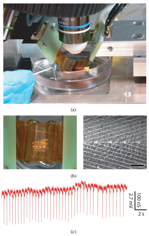
(a) (Yellow arrow) Heart located underneath bent substrate with NWFETs on the lower concave face of the substrate. (b, left) Top-down photograph of same system, which enables overall registration between heart and lithographically defined markers on the substrate. (Right) Optical image taken with same system showing features on the heart surface versus position of individual NW devices, which are located along the central horizontal axis. Scale bar is 150 μm. (c) Recorded conductance data from an NWFET in the configuration shown in (a). Adapted from [56] (American Chemical Society, copyright 2009).