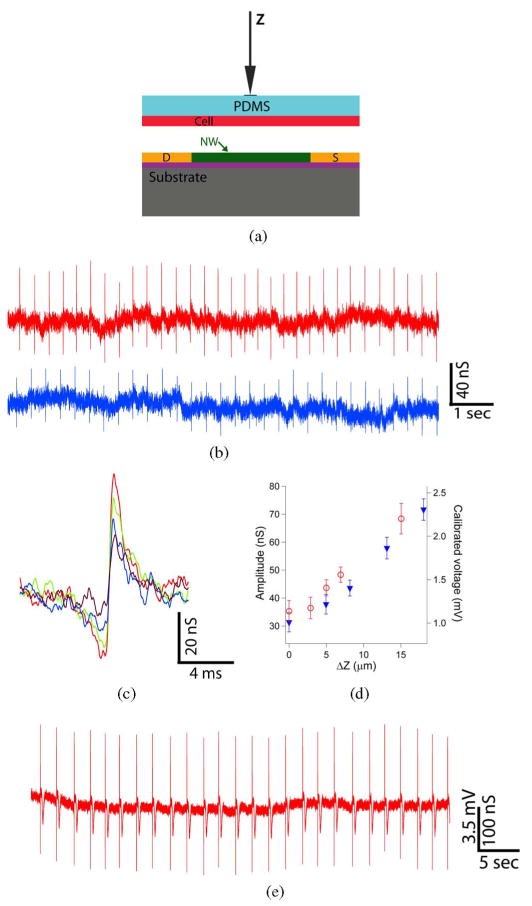
Fig. 13.

(a) Schematic illustrating displacement (Z) of the PDMS/cell substrate with respect to an NWFET device. (b) Two representative traces recorded with same device for ΔZ values of (blue) 8.2 μm and (red) 18.0 μm. (c) High-resolution comparison of single peaks recorded with ΔZ values of (purple) 0, (blue) 8.2 (blue), (green) 13.1, and (red) 18.0. (d) Summary of the recorded conductance signals and calibrated voltages versus ΔZ, where the open red circles (filled blue triangles) were recorded for increasing (decreasing) ΔZ. (e) Data recorded in distinct experiment at ΔZ close to cell failure. Adapted from [73] (National Academy of Sciences, copyright 2009).
