
Fig. 4.
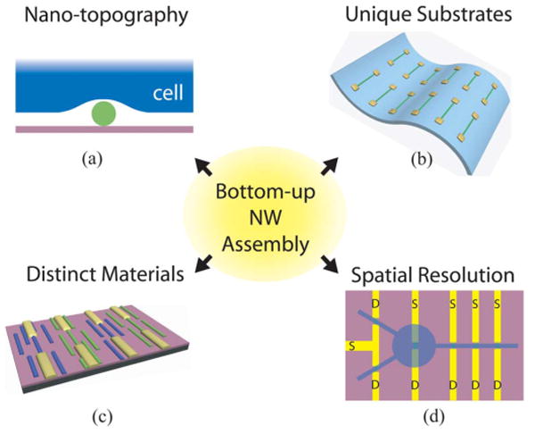
Schematic diagram outlining unique advantages of bottom-up NW assembly, including (a) nanotopographic morphology, (b) ability to assemble devices on flexible, transparent substrates, (c) assembly of distinct NW materials on the same chip, and (d) high spatial resolution of NW devices, where S and D correspond to source and drain electrodes.