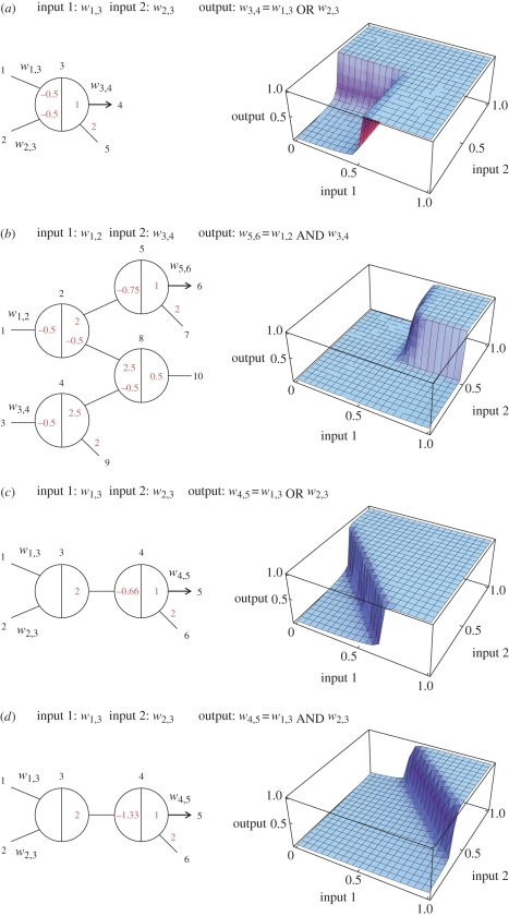
Figure 3.
Circuit diagrams and input/output behaviour of boolean logic gates. Output wires with arrowheads indicate that a downstream load is assumed, which consumes signal strands as they are released. (a−b) A two-input OR gate and a two-input AND gate using, respectively, 1 and 4 seesaw gates, the ‘1-4 scheme’. Circuits constructed using the 1-4 scheme are not clean, and thus would perform worse if threshold crosstalk and threshold inhibition were modelled. (c–d) A two-input OR gate and a two-input AND gate using two seesaw gates each, the ‘2-2 scheme’. Circuits constructed using the 2-2 scheme are clean. All simulations were performed with the reference concentration 1x = 50 nM, and stopped at t = 10 h. Here and in all other simulations, kf = 2 × 10⁶ M−1 s−1 and ks = 105 M−1 s−1.

