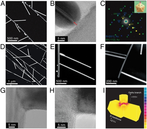
Fig. 2.
Structural characterization of type I branched NW heterostructures. (A) SEM image of Si/Au branched NWs. (B) HRTEM image of Si/Au branched junction; red arrow highlights twin plane. (C) SAED pattern of the junction region shown in B, where blue and green spots originate from 〈100〉Au, 〈112〉Au zone diffraction, and yellow spots are from the crystalline Si backbone. (Inset) Cross-sectional model of the penta-twinned Au branch consisting of five twinned subunits. Red arrow marks the incident beam direction. (D–F) SEM images of Si/Ge (D), Si/GaAs (E), and Si/GaP (F) branched NWs. (G and H) HRTEM images of Si/Ge (G) and Si/GaAs (H) branched junctions. (I) Simulated von Mises stress field at Si/GaAs branched junction. The scale bar range is from 3.1 × 10⁶ to 1.6 × 10¹⁰ Pa.

