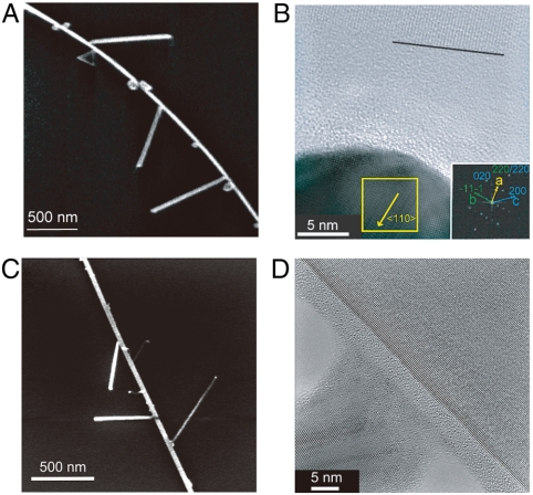
Fig. 3.
Structural characterization of type II branched NW heterostructures. (A) SEM image of Si/SiO2/Au branched NWs. (B) HRTEM image of Si/SiO2/Au junction. The black line marks the SiO2/Si interface. (Lower Right Inset) FFT pattern from the yellow square region, indexed as a superposition of [001] (blue) and [-112] (green) zone patterns. The marked yellow spot in the FFT pattern is one of the associated double diffraction reflections, where a = b + c. (C and D) SEM (C) and HRTEM (D) images of Si/SiO2/Ge branched NW.

