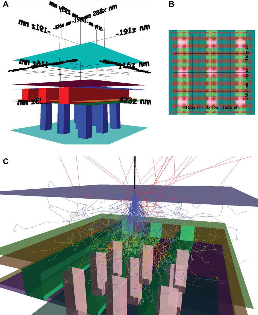
Figure 1.
Screenshots from CASINO software of a 3D sample. A: 3D view of the sample showing the different shapes and regions. B: Top view of the sample with the scan points used to create an image. C: Electron trajectories of one scan point with trajectory segments of different color for each region. The sample used is a typical CMOS stack layer for 32 nm technology node with different dielectric layers, copper interconnects and tungsten via.

