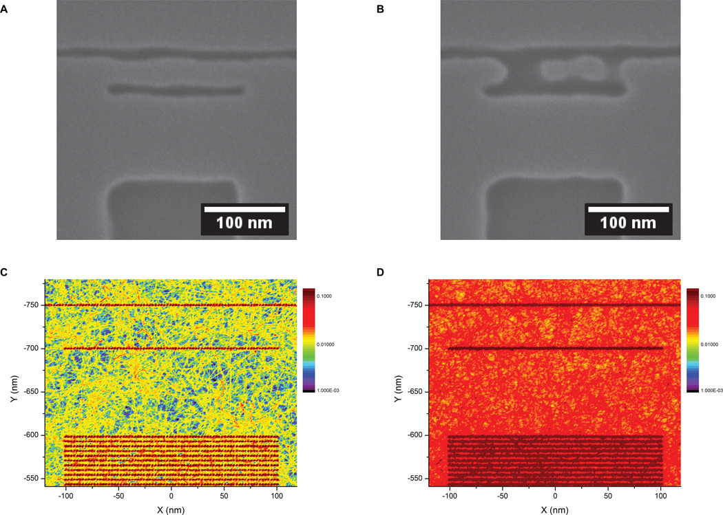
Figure 7.
Simulation of the electron dose effect on electron beam lithography. Two experimental secondary electron images, after electron beam lithography, where the pattern was A: successfully developed and B: incorrectly developed. C: and D: top view of the energy absorbed in the resist from the electron beam pattern simulated with CASINO. The number of electrons per scan point was: C: electron dose of 130 µC/cm2 and D: electron dose of 700 µC/cm2. The energy absorbed is normalized and displayed on a logarithmic scale.

