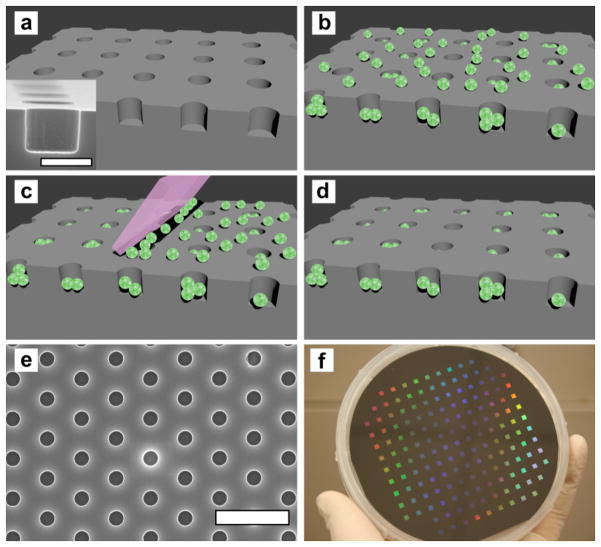
Figure 1.
Schematic illustration of the array assembly process and images of microwell substrates. (a) Illustration of an array of wells in an Al2O3-coated silicon substrate. Inset: A cross sectional SEM image of a microwell. The scale bar is 1 μm. (b) Vesicles are deposited on the substrate and fill the wells as well as populate the top surface. (c) The PDMS block “squeegee” is translated across the substrate, removing vesicles that are not immobilized in the recessed wells. (d) After using the squeegee, the top surface of the substrate is devoid of vesicles, while the recessed wells are filled. (e) SEM image of a hexagonal microwell array with 1 μm well diameter and 3 μm periodicity. The scale bar is 5 μm. (f) Photograph of a 4 inch wafer patterned with 157 microwell arrays, each with 1 μm well diameter and depth and 3 μm periodicity.

