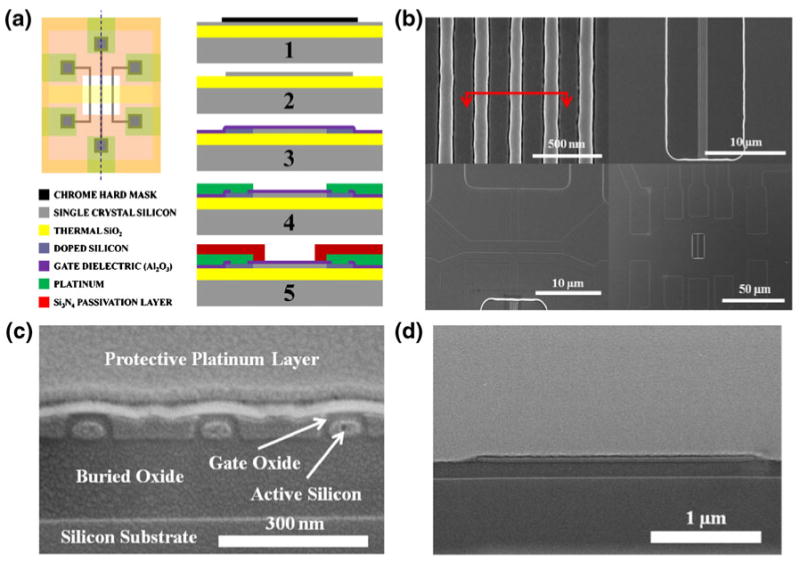
Fig. 1.

Device structure. (a) Fabrication process for the Nano-FETs. 1—Patterning of chrome hard mask via electron beam and optical lithography. 2—Wet Etch of the active silicon area with TMAH. 3—Deposition (Al2O3) or growth (SiO2) of the gate dielectric. 4— Deposition and patterning of platinum as the metal contact; contact is made with via holes into the silicon. 5—Deposition of Si3N4 passivation layer, followed by etchback to expose the devices and the fluid gate. (b) Scanning electron micrographs of NW-FETs, demonstrating how mesas are used to make contact to the wires and to the metal traces. (c) SEM of a cross section of three NW-FETs (through the red line in part b). A protective platinum layer was placed over the cross section to prevent damage to the surface while taking the cross-section. (d) SEM of a cross section of a single nanoplate FET
