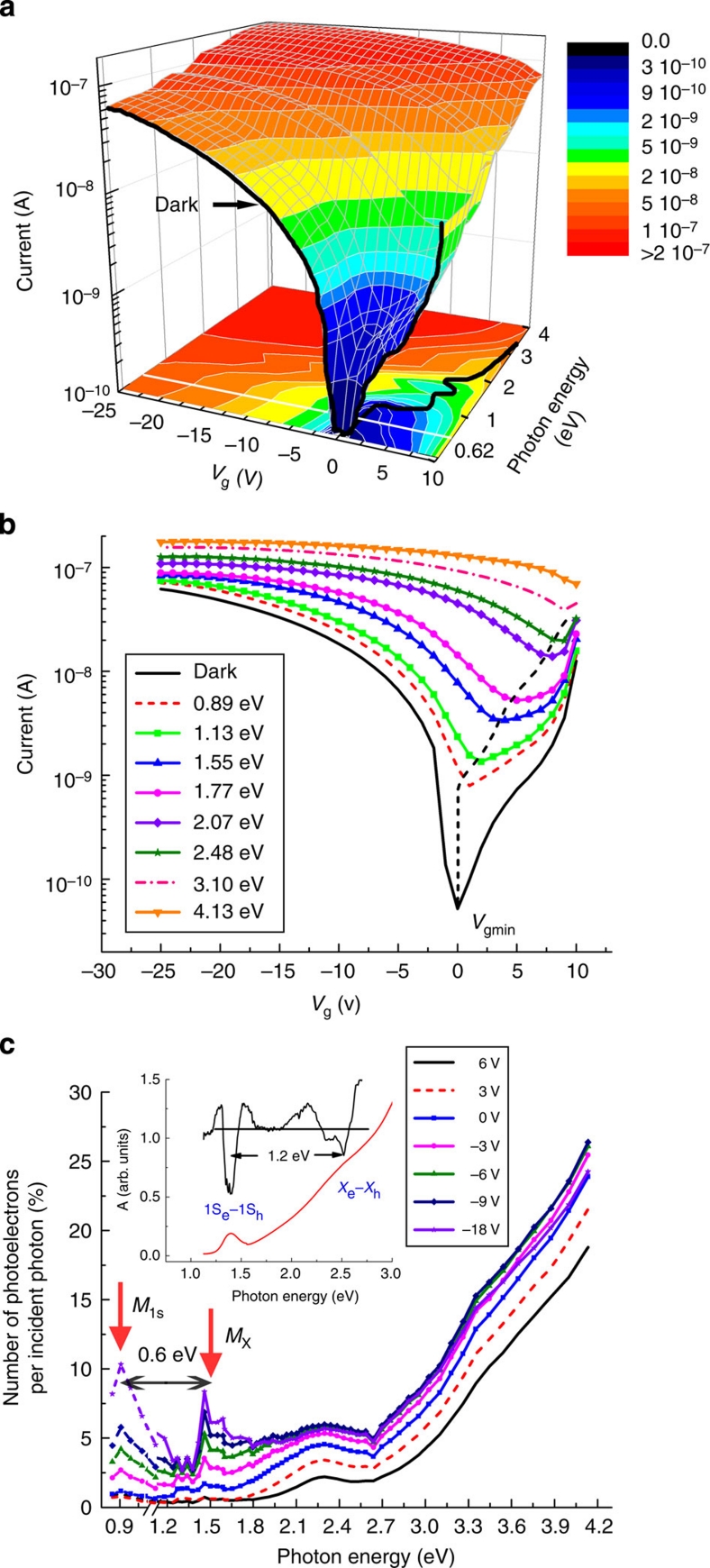
Figure 2. Spectrally resolved responses of OFET indicate presence of mid-gap states forming weakly conductive band.
(a) Isd-versus-Vg characteristics obtained in dark (black line) and under illumination as a function of photon energy starting from 0.62 eV (white line in the contour plot at the bottom). Coloured filling below the white line is interpolation between the measurements in dark and under 0.62 eV illumination. Black line in the contour plot at the bottom traces changes in the flat-band potential. (b) 'Cross-sections' obtained from the three-dimensional plots in panel 'a' show the variation of the source–drain current as a function of gate voltage under illumination at different photon energies (shown in the legend). (c) Photocurrent as a function of incident photon energy shown in terms of the number of photoelectrons per 100 incident photons (derived from data in panel 'a'). The spacing between the two prominent features (M1S and MX), that develop under negative bias, is half of the spacing between the 1S and X features in the second-derivative of the absorption (A) spectrum (inset). This suggests that the M1S and the MX peaks are likely due to transitions between the occupied 1S and X valence band states and the unoccupied MGB states, respectively.

