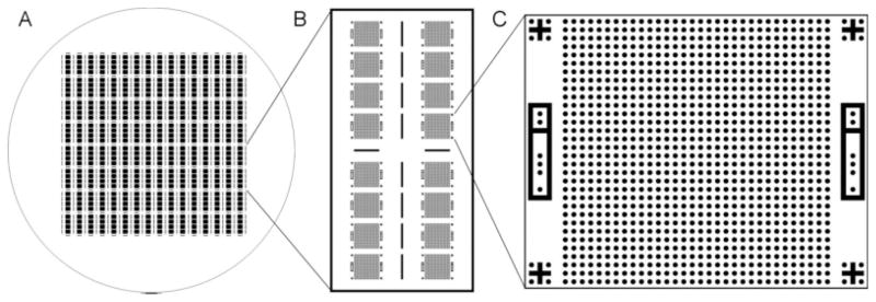
Figure 1. A reusable mold for casting the PDMS devices is fabricated on a 4 inch silicon wafer using photolithography.
As seen in Panel A, each wafer contains 512 microwell arrays arranged in groups of four and separated by cutting guides. Each PDMS sheet is typically divided into 32 devices measuring 1.6 × 0.8 cm for easy mounting on mini glass slides. As shown in Panel B, each device contains 16 individual arrays with an empty region at the center for pipetting. In some experiments, half sized devices with eight arrays were used to allow for faster imaging. Panel C shows the layout of a typical array, including a regular 32 × 32 grid of 25 μm wells designed to hold single cells, alignment features at each corner, and unique binary identification features on each side.

