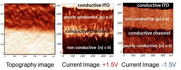
Figure 4.

AFM pictures taken on a cleaved section of an ITO/(p) a-Si:H/(n) c-Si/ITO sample. Left: topography; middle: current image taken at an applied bias of +1.5 V. Right: current image taken at an applied bias of -1.5 V. Typical roughness was less than 5 nm. On the topographical image, the change in height from the dark top region to the light bottom region was of the order of 2 nm. In the current images, the current values ranged from 60 pA to 17 nA.
