Figure 5.

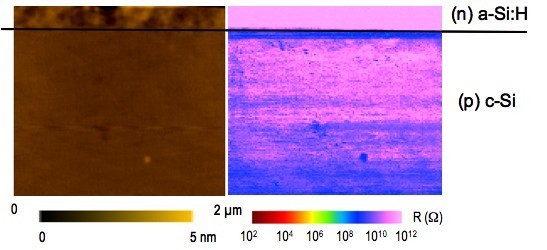
Topography and electrical image obtained after HF dip at the cleaved section of an (n) a-Si:H/(p) c-Si heterojunction. Left: topography; right: resistance image.

Topography and electrical image obtained after HF dip at the cleaved section of an (n) a-Si:H/(p) c-Si heterojunction. Left: topography; right: resistance image.